PCB Manufacturing Explained: Step-by-Step Process, and Quick-Turn Industrial Solutions
Printed circuit boards (PCBs) are the foundation of every electronic product — from medical sensors and cars to industrial controllers and smartphones.
This article walks you through the entire PCB manufacturing process, explains what really affects cost, and shows how industrial-grade quality and quick-turn manufacturing come together to deliver reliable boards, on time.
PCB Manufacturing Process — From Design to Final Inspection
Every PCB, whether a simple two-layer prototype or a 30-layer HDI board, goes through a series of controlled steps. Each stage affects the board’s precision, durability, and price.
1. Data Preparation and DFM
Everything begins with your design files — usually in Gerber, ODB++, or IPC-2581 format.
The factory’s engineering team checks for manufacturability: layer stack-up, trace width and spacing, drill sizes, and solder-mask clearance.
A quick Design for Manufacturability (DFM) review at this stage prevents issues later.
2. Inner Layer Imaging and Etching
Copper foil is laminated to a dielectric base and coated with photoresist film.
Using UV light exposure or a laser direct imaging (LDI) machine, the circuit pattern is transferred onto the copper.
Unwanted copper is chemically etched away, leaving clean traces and pads.
Alignment between layers is carefully controlled to maintain accuracy.
3. Lamination
Multiple inner layers are stacked with sheets of prepreg (semi-cured resin) and pressed together under heat and pressure.
This forms the multilayer PCB core.
Proper lamination ensures resin flow and bonding between layers without voids or delamination.
4. Drilling and Via Formation
Next comes drilling.
Mechanical drills create through-holes for component leads and vias.
Laser drilling is used for microvias in HDI designs.
After drilling, holes are cleaned and roughened (“desmear”) so copper can adhere well during plating.
5. Copper Plating and PTH
A thin chemical copper layer is deposited inside the holes, followed by electroplating to increase thickness.
This connects all layers electrically.
Process control is critical — inconsistent plating can cause open vias or cracks under thermal stress.
6. Outer Layer Imaging and Pattern Plating
The outer layers are imaged and plated the same way as the inner layers.
Copper is plated on traces and pads, and a thin tin layer protects the circuitry during final etching.
After etching, only the designed circuit pattern remains.
7. Solder Mask and Silkscreen
A green (or sometimes black, white, or blue) solder mask is applied to protect copper and prevent solder bridges.
Openings are created for pads where components will be soldered.
Then, component reference text and logos are printed using silkscreen or inkjet methods.
8. Surface Finishing
Surface finish protects exposed copper and ensures solderability.
The most common types include:
- HASL (Hot Air Solder Leveling): economical but not ideal for fine-pitch parts.
- ENIG (Electroless Nickel Immersion Gold): smooth, flat, and suitable for BGA and fine-pitch.
- ENEPIG: adds a palladium layer for better wire bonding.
- OSP (Organic Solderability Preservative): low cost, good for short shelf life.
- Immersion Silver/Tin: great for lead-free production.
Choosing the right finish depends on assembly needs, storage time, and budget.
9. Profiling, Testing, and Final Inspection
After finishing, panels are routed or punched into individual boards.
Each PCB is electrically tested by flying-probe or fixture to ensure no shorts or opens.
Automatic Optical Inspection (AOI) checks every trace and pad.
Finally, boards are cleaned, packaged, and labeled for traceability.
10. From Fabrication to Assembly
The finished bare board moves into assembly (PCBA).
Solder paste is printed, components are placed, and reflow soldering creates reliable joints.
X-ray inspection verifies BGA and QFN solder quality.
Designers who consider assembly rules early — pad sizes, via spacing, thermal relief — avoid rework later.
Industrial PCB Manufacturing: Quality, Capacity, and Compliance
When moving from lab-scale builds to industrial production, consistency and certification matter more than ever.
1. Automation and Process Control
Modern PCB plants use high-precision imaging (LDI), automatic etching lines, and in-line AOI to monitor each stage.
Statistical Process Control (SPC) tracks parameters like plating thickness, temperature, and humidity.
Full traceability — from raw materials to finished lots — supports reliability and accountability.
2. Quality and Certifications
- Industrial customers expect proven compliance.
Key certifications include: - ISO 9001 for quality systems
- ISO 13485 for medical applications
- IATF 16949 for automotive
- UL, RoHS, and REACH for safety and environmental compliance
- IPC-A-600 / IPC-6012 for acceptability standards
For example, FastTurn PCBs manufactures under ISO 9001 and 13485 quality systems, serving sectors such as medical, industrial control, and communications.
Consistent process documentation and material traceability help reduce risk across the supply chain.
3. Industry-Specific Requirements
- Each industry has unique reliability targets:
- Automotive: high-Tg materials and via fatigue testing under heat cycles.
- Medical: cleanroom standards, traceable materials, and lot-level documentation.
- RF/Microwave: low-Dk/Df laminates and controlled surface roughness for signal integrity.
- Industrial control: insulation strength and vibration resistance.
A capable fabricator understands these nuances and adjusts stack-up, plating, or surface finish to match application needs.
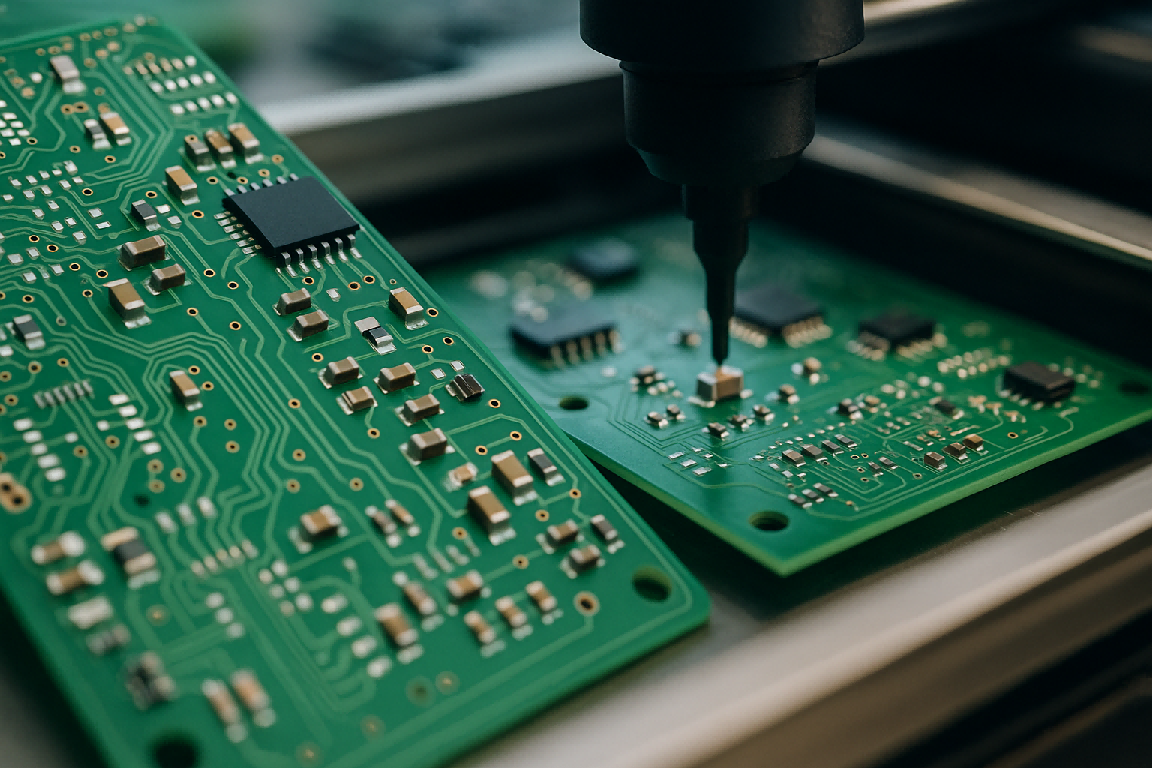
Machines Behind PCB Manufacturing
Every stage of PCB fabrication relies on precise equipment:
- LDI exposure machines for accurate imaging
- Automatic lamination presses for multilayer bonding
- High-speed CNC and laser drills for vias and microvias
- Chemical copper and electroplating lines
- Solder mask inkjet or screen printers
- Routing/CNC profiling systems
- AOI, flying-probe testers, and X-ray machines for inspection and testing
Together, these tools ensure the consistency and repeatability required for today’s dense, high-layer-count boards.
How to Choose the Right PCB Manufacturer
Finding the right manufacturing partner is more than comparing prices.
Look for:
- Proven certifications (ISO, UL, IPC) and real production experience.
- Capabilities that match your design — HDI, rigid-flex, high-frequency, or heavy-copper.
- Fast, clear engineering communication and responsive DFM support.
- On-time delivery and quality statistics, not just promises.
- Smooth transition from prototype to mid-volume production.
If you value fast turnaround with reliable quality, consider working with a provider like FastTurn PCBs, which offers multilayer and high-frequency fabrication as well as turnkey PCB assembly under one roof.
This saves coordination time and reduces the risk of mismatch between the fab and assembly stages.
Summary
PCB manufacturing combines precision chemistry, mechanical control, and engineering skill.
By understanding each stage — from imaging and drilling to finishing and testing — designers can make better technical and cost decisions.
When choosing a manufacturing partner, look for one that balances speed, quality, and communication.
FastTurn PCB offer a strong combination of quick-turn prototyping, industrial-grade reliability, and turnkey PCB assembly, helping engineers move from concept to production faster and with fewer risks.